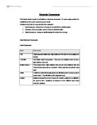
Passive Components
Components are said to be Passive if they are unable to provide any power amplification. This means that components such as resistors, capacitors, normal diodes, LEDs etc. are described as passive. Section 6.2 deals with active components, which are able to provide power again. These include such devices as transistors and MOSFETs.
They are however, the only way to obtain large value capacitors that are physically small. Capacitors made from Tantalum have better characteristics than normal electrolytic capacitors but are considerably more expensive.
Electrolytic capacitors are mainly used for smoothing and decoupling (removal of low frequency signals) from power supplies. Wherever possible, their use in the signal path of circuits should be avoided so as to minimise signal distortion. Non-polarised capacitors should be used instead.
Uses of resistors
- Limiting the current flow through a device e.g. LED, zener diode, base of a transistor,
- Converting a current flow into a voltage
- Converting a voltage into a current
- Voltage divider circuits,
- With capacitors as charging and discharging circuits
Uses of capacitors
- Smoothing out variations in power supplies
- Removing alternating signals
- Blocking the passage of direct current while allowing the passage of alternating current
- Combination with inductors for resonant tuned circuits
- Combination with resistors as charging and discharging circuits
Diodes
A diode is a semiconductor device that only allows current to pass one way. The symbol for a diode is shown in figure _____, the direction of the arrow indicating the direction of the conventional current flow from anode to cathode.
When a diode passes a current from anode to cathode the anode is positive with respect to the cathode and the diode is said to be forward biased.
When the cathode of a diode is positive with respect to the anode then no current is able to flow and the diode is said to be reverse biased.
Light-emitting diode (LED)
A LED is a diode made from the semi-conductor gallium arsenide phosphide. Its component outline and symbol are shown below. When forward biased it conducts and emits light of a certain colour depending on its composition. No light emission occurs in reverse bias and if the reverse voltage exceeds approximately 5V then the LED may be damaged.
A LED requires a series resistor to ensure the current does not exceed its maximum rating, which should be taken as 20mA. The forward voltage drop across a LED is about 1.8V, though it does depend upon the colour of the LED.
To calculate the value of the series resistor it is first necessary to decide on the current that should flow through the LED. The data sheet for the LED will specify a maximum current Imax. The LED current should be less than this. If the supply voltage is Vs, then
Vs – 1.8
R = Imax
The minimum value used for R should be the next largest preferred value.
LEDs are used as indicator lamps and in seven-segment displays. They have the advantages of small size, long life, a small operating current and high operating speed. There is now a large range of different LEDs available with outputs ranging from the infrared to blue wavelights.
Seven segment array
Electronic calculators, clocks, cash registers and measuring instruments often have seven-segment LED displays as numerical indicators. Each segment is an LED and by lighting up different segments all numbers from 0 to 9 can be displayed. Each segment needs a separate current limiting resistor to prevent damage to the segment by excess power dissipation.
All the cathodes (common cathode type) or all the anodes (common anode type) are joined to form a common connection. If the driving circuit is made from transistors, so that the seven-segment display segments are connected in the collector circuits, then a common anode Figure ____ display will be required.
Seven segment Display
Seven-segment LED displays consist of seven small LEDs arranged to produce the decimal numbers 0-9 when different combinations of the segments (LEDs) light up.
If the LED cathodes are linked together then they are known as the common cathode displays, that means that the common cathode connection would be linked to 0V and when each of the segments have high inputs they will light up.
Logic Gates
Combinational logic.
Digital electronics is concerned with switching-type circuits in which the inputs and outputs involve only to levels of voltage (or current). Digital information (signals) therefore consists of a series of voltage pulses, with HIGH voltage being represented by a 1 and a LOW voltage being represented by a 0.
Digital circuits consist of logic gates, which control the flow of digital information. A logic gate is a device, which has one output and several inputs. The output will either be a logic 1 (high) or a logic 0 (low) depending on the input signals. The logic gates covered in the syllabus are assumed to have a very high input resistance, and a low output resistance. Logic 0 is assumed to be less than half of the supply voltage and logic 1 is assumed to be more than half of the supply voltage. These are the characteristics of the CMOS, 74HC and 74 HCT logic families.
All of these logic circuits will operate from a well-regulated +5V supply and it is assumed in circuit diagrams that a power supply is connected even though the connections will not be shown.
Analogue electronics uses continuously varying voltages and so it is not possible to produce tables showing the relationship between very possible input and output, the tables would be infinitely long. Digital electronics, however, having only two states for each input, does not have this problem. Tables showing the relationship between inputs and output can be readily constructed for digital circuits. These are known as TRUTH TABLES.
There are three basic logic functions or gates: AND, OR and NOT.
ALL digital electronic circuits are built from combinations of these basic gates.
AND Gate
Astable generators; the 555 timer
This is very versatile integrated circuit was first produced in 1973. The circuit and its derivatives are still used in large quantities. While it is not necessary to know the internal structure of this device, it does aid understanding if the main internal features are known. These are as follows:
- Three precision resistors arranged across the power supply as a voltage divider and so giving voltages of 1/3 Vs and 2/3 Vs is the supply voltage;
- Two comparators, one switching at 1/3 Vs via the TRIGGER input and the other switching at 2/3 Vs via the THRESHOLD input;
- A latch, SET by the output of the TRIGGER comparator and RESET by the output of the THRESHOLD comparator;
- A high current output capable of sinking or sourcing 200mA;
- An open collector transistor switch, which connects the DISCHARGE terminal to 0V when the output terminal at 0V.
The pin diagram for 555 timer IC is shown in figure
PICTURE OF 555
The operation of a 555 can be summarized as follows.
- If the voltage at the TRIGGER input is less than 1/3 Vs then the output goes to Vs and remains there until the voltage at the THRESHOLD input rises above 2/3 Vs, at which value the output is set at 0V.
- The RESET terminal can be used to set the output to 0V at any time by being connected momentarily to 0V. Normally, the RESET terminal is connected to Vs to prevent any spurious resetting of the output.
-
The CONTROL terminal is connected to the 2/3 Vs point of the voltage divider and can be used to alter the voltage switching levels of the comparators. Normally it is decoupled by a 10nF capacitor connected to 0V.
The 555 astable
The common circuit for a 555 astable is shown in figure
When first switched on the capacitor, C, is discharged and so the voltage across this capacitor is less than the TRIGGER voltage and so the output goes to Vs. The capacitor, C, charges through R1 and R2 until the voltage across C is greater than the THRESHOLD switching level, at which point the output voltage becomes 0V and the DISCHARGE terminal becomes connected to 0V.
The capacitor now discharges through R2 until the voltage across C becomes less than the TRIGGER switching voltage. When this happens, the output voltage becomes Vs and the process repeats. It should be noted that the first pulse is longer than the remainder, since C has to charge from 0V and not 1/3 Vs. The same restrictions apply to the values of C and R (R1 and R2) as for the monostable.