The other characteristic is the sampling rate. This is also known as the speed at which the converter executes its operation. To obtain an accurate sample of a signal it is necessary to use the Nyquist sampling rate which is defined to be twice the maximum frequency of the input signal. Any sampling rate less then this would lead to a spurious signal. High frequency signals were not introduced in these experiments.
These characteristics determine and differentiate converters on the market. Analogue-to-Digital converters are being used more and more in today’s world due to the fact that it’s easier and more accurate to transfer from one point to another.
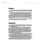
Digital-to-Analogue Conversion
Digital-to-Analogue converters take digital inputs and convert them into an analogue signal. The converters used are parallel converters as they accept the whole digital number presented and not each bit at a time. The basic principle behind DAC is that the output is a binary-scaled sum of voltages or currents. The least significant bit (LSB) should have a weight much lower than the most significant bit(MSB). (Refer to Appendix A for further information).
The circuit used for this experiment was the R/2R Ladder network (Figure 1). By analysing the circuit (Appendix B), it is clear that the accuracy of the converter depends on the ratio of the resistors and not on their actual value. This is an important factor as ratios are much better controlled then absolute values.
Figure 1: R/2R Ladder Network
Experimental procedure
1 - A 4-bit converter was constructed in accordance with figure1. Vr was set to 8 volts and the difference between levels would be -0.5V.
2 - Resistors were used in parallel to obtain the required ratio and values. The ideal resistor value was obtained by trial, making sure that the drop of the MSB was not more than 0.2LSB. RF = R and Rc = R//RF .
3 - Input numbers from 0 to 15 were evaluated and measured (figure 2).
4 – Sensitivity was measured by making small changes in the resistor of the MSB. It is defined as the change in output as a percentage of full scale, divided by the percent change in the value of the resistor (Table 1).
5 – Using the counter, display a dynamic ramp, clock signal of counter around 500Hz (Figure 3). Then by changing the MSB resistor, produce a non-monotonic response. The derivation to see if it agrees with theoretical values is presented in the appendix C.
6 – Estimate settling time of the output voltage from full scale to zero
7 – Modify the converter to support two’s complement binary inputs.
Experimental Results
2 – The value of the resistor obtained was 15kΩ. Rc would then be 7.5kΩ.
3 – The values obtained are negative due to the inverting amplifier used.
Figure 2 - Voltage level of inputs from 0 to 15.
4 - The set output voltage used was -7,477. The value used for comparisons.
Table 1 – Relationship between change in output and change in resistor values for a full scale operation.
5 –
Ramp sasdf dsafasdf adf
6 – The settling time was seen to be around 6us. By looking at the negative inverting input of the opamp, a glitch is visible. This shows that the virtual earth does not work at all times. When the input changes from 1111 to 0000 the internal capacitor has to discharge and charge again to achieve zero.
7 – In order to modify the converter to except two’s complement the ladder network was altered as well as the amplifier. A differential summing amplifier was used (figure 6). The ladder network (Figure 1) was connected to this amplifier so that point P was connected to the VA input of the amplifier. This would invert the MSB to take into account any negative values.
Figure 6 – Differential summing amplifier
Analogue-to-Digital Conversion
Analogue-to-Digital converters are common and therefore are very diverse between them. The choice of which converter to choose normally involves the decision of what factors are more and least important for the job. These factors are speed, accuracy and power consumption. ADCs output and estimate of what the output is and then compares it back with the actual input signal. It will continue to do this until an ideal estimate has been found. One of the converters used was the Ramp converter (Figure 7). This method uses a digital counter to count upwards starting from zero, which goes through a DAC and compares it to the input signal. When the number is reached by the counter, it stops and our digital number is found. For this to occur accurately, there has to be sufficient time for the number to be converted from digital to analogue and compared with the input signal before continuing counting. The zener-diode is used to pull down any current from going into the nand gate. The counter shows the nearest equivalent digital value to Vin rounded up due to the fact that the value from the DAC is marginally greater than Vin.
Figure 7 – Ramp Converter
Experimental Procedure
1 – Using a clock frequency of 5 kHz and a high order bit to provide a counter for the repeating reset command, find the range of dc input voltages corresponding to each digital value and explain any offsets.
2 – Increase clock frequency and find maximum clock frequency at which converter operates correctly. What happens when the frequency exceeds this limit and why ?
Experimental Results
1 – This table is the result from the experiment done. Any voltage in between the lower and upper limit will be equal to the corresponding number.
Table 2 – Upper and lower limits for each number.
2 – The maximum frequency of the converter is 32.1 kHz. The slew rate is the time taken for the output of the amplifier to respond to a change in input, it’s the maximum frequency that the amplifier can operate. The clock period is inversely proportional to the frequency so when the period becomes smaller then the slew rate, it is unable to stop the counter quickly enough so the counter will count one or more values above the correct value until it’s stopped.
Successive Approximation Converter
The ramp converter is clearly not an ideal converter as the conversion time depends on the amplitude of Vin and can take up to 2n-1 clock cycles for an n-bit converter. The successive approximation converter is more intelligent and faster, operating at 1 to 10 usec per bit. In this case, the converter performs a binary search for Vin, starting at the midpoint range and asks the comparator which way to go next. The main advantage of the successive approximation converter to the ramp converter is the fact that the ramp converter starts it’s initial count at zero whereas the successive approximator converter starts at a number obtained from a special shift register, Successive Approximation Register (SAR) (Appendix D).