- Flags register is used to record the effect of the last ALU operation
- Instruction register is used to hold the instruction that is currently being executed. When an item of data is identified as an instruction, it is transferred to the IR prior to being decoded and executed. It is also known as the Current Instruction Register (CIR)
- Program Counter or sequence control register (PC) holds the address of the next instruction to be fetched. After an instruction has been fetched, the PC is automatically incremented by one (sometimes more). It is also altered by certain types of instructions (jumps). It can be altered by the programmer to start program execution from a different address.
-
Memory Address Register (MAR) holds the address of the data (or instruction) currently being accessed. It is directly connected to the address bus.
-
Memory Buffer Register (MBR) holds the contents of the last data that was either read from or written to the main memory. It is directly connected to the data bus.
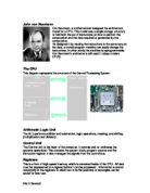
A typical layout shows the data paths.
The fetch/execute cycle
When the computer is turned on it starts performing what is known as the fetch/execute cycle. It is the job of the microprocessor which is controlling the computer to fetch a single program instruction from the memory, decide what to do (by decoding this instruction), and then carry out any action which might be needed (execution of this instruction).
It is the sole task of the microprocessor to carry out this fetch-decode-execute cycle over and over again operating on different instructions from memory. It does nothing more and nothing less. This fetch-decode-execute cycle is often shortened to the fetch-execute cycle as the decoding is done within the fetch part by some electronic chips.
The fetch/execute cycle consists of the following steps:
- Fetch
- Decode
- Execute
Fetch
(1) The processor copies the contents of the program counter into the MAR
(2) The instruction is transferred via the data bus to the MBR
- The contents of the MBR are copied into the instruction register
Decode
The instruction in the instruction register is decoded.
IF the instruction turns out to be a JUMP instruction THEN
The address part of the instruction is put into the PC
The cycle is reset and another fetch-decode-execute cycle begins
ELSE
Execute the instruction
Reset the cycle by going back to the beginning of fetch-decode-execute cycle.
ENDIF
Overview of steps in executing a program
Steps involved in executing 1st instruction:
Fetch Cycle
- PC is set [120]
- Contents of PC [120] is copied to MAR
- PC is incremented to [121]
- Control unit sends a read signal to memory address with address in MAR
- Data from memory sent to CPU on data bus and set MBR
- CPU checks whether it is an instruction. The contents of MBR is copied to CIR and is decoded.
At this stage, the CPU knows it has to go to address [10] and transfer its contents to Accumulator
Execute cycle
- MAR is set to [10]
- Control unit sends a read signal to memory address to read contents of [10]
- Data from memory sent to CPU on data bus and set MBR
- CPU copied the contents of MBR to Accumulator.
Steps involved in executing 2nd instruction:
Fetch Cycle
- Contents of PC [121] is copied to MAR
- PC is incremented to [122]
- Control unit sends a read signal to memory address with address in MAR
- Data from memory sent to CPU on data bus and set MBR
- CPU checks whether it is an instruction. The contents of MBR is copied to CIR and is decoded.
Execute cycle
- MAR is set to [11]
- Control unit sends a read signal to memory address to read contents of [11]
- Data from memory sent to CPU on data bus and set MBR
- Control unit sends a signal to ALU that an ADD operation is to take place.
- CPU transfers the contents of Accumulator to one register (let be REG for explanation) inside the ALU
- CPU copied the contents of MBR to Accumulator.
- CPU adds the contents of register ‘REG’ with Accumulator in a register in ALU and overwrites the old value of accumulator with the answer.
Steps involved in executing 3rd instruction:
Fetch Cycle
- Contents of PC [122] is copied to MAR
- PC is incremented to [123]
- Control unit sends a read signal to memory address with address in MAR
- Data from memory sent to CPU on data bus and set MBR
- CPU checks whether it is an instruction. The contents of MBR is copied to CIR and is decoded.
Execute cycle
- MAR is set to [12]
- The contents of the Accumulator is transferred to MBR
- Control unit sends a write signal to memory address to write to the address [12]
Data from CPU sent to memory on data bus to address [12]
Comparison of Von Neumann processors:
The clock determines the timing for all operations and is used to synchronise the computer system. If the clock runs at a higher speed each operation will take less time and so the performance will be enhanced. A faster clock increases the speed of the processor but not the peripherals. The faster the clock, the more FDE cycles can be performed.
A CPU sends and receives information in the form of bits. The number of bits it can send or receive in one go from memory or I/O along the computer’s data bus is known as the ‘word size’. The bigger the word size, the faster the computer can work on data. Consider a 32-bit number is stored in memory, a 32-bit computer could fetch this number in one clock cycle. A 16-bit computer in 2 clock cycles. An 8-bit computer in 4 clock cycles. The bigger the word size, the faster your computer!
A wider bus will allow more bits to be transferred at one time. There have been computer systems produced where the registers were larger than the bus width. This gave high-speed calculations but the transfer of data was slow owing to the number of transfers that had to take place. Larger data buses improve data flow between the memory and the processor.
- Pipelining is a technique that exploits parallelism among the instructions in a sequential instruction stream.
Definition : A Pipeline is a series of stages, where some work is done at each stage. The work is not finished until it has passed through all stages. Pipelining is an implementation technique in which multiple instructions are overlapped in execution. Today, Pipelining is key to making processors fast. A pipeline is like an assembly line: in both, each step completes one piece of the whole job. Workers on a car assembly line perform small tasks, such as installing seat covers. The power of the assembly line comes from many cars per day. Note that the assembly line does not reduce the time it takes to complete an individual car; it increases the number of cars being built simultaneously and thus the rate at which the cars are started and completed. There are two types of pipelines, Instructional pipeline where different stages of an instruction fetch and execution are handled in a pipeline and Arithmetic pipeline where different stages of an arithmetic operation are handled along the stages of a pipeline. Each stage can operate independently.
Suppose a pipeline which the capacity of doing three different parts of the cycle (fetch, decode, execute) at once. By the end of the third cycle, the first instruction has been fetched, decoded and executed, the second has been fetched and decoded, and the third one has been fetched.
Disadvantages of pipeline architecture
- Complexity.
-
Inability to continuously run the pipeline at full speed, i.e. the pipeline stalls. There are many reasons as to why pipeline cannot run at full speed. There are phenomena called pipeline hazards, which disrupt the smooth execution of the pipeline. The resulting delays in the pipeline flow are called bubbles. These pipeline hazards include
- data hazards arising from data dependencies
- Control hazards that come about from branch, jump, and other control flow changes
Von Neumann bottleneck
Whatever you do to improve performance, you cannot get away from the fact that instructions can only be done one at a time and can only be carried out sequentially. Both of these factors hold back the efficiency of the CPU. This is commonly referred to as the ‘Von Neumann bottleneck’. You can provide a Von Neumann processor with more RAM, more cache or faster components but if major gains are to be made in CPU performance then a fundamental review needs to take place of CPU design.
Parallel Processor Systems
Parallelism is:
- at least 2 processors working together,
- more processors can give faster execution,
- Breaking up the task into smaller tasks (partitioning the task)
- Assigning the smaller tasks to multiple workers(processors) to work on simultaneously
- Coordinating the workers (processors)
Reasons for parallel processing:
- Programs that are too large for available serial architectures.
- Processing that would take too long to execute on serial machines.
- Don't handle large loads well, e.g., a database server which operates well with 10 users, but when 100 people use it the performance suffers.
Pipelining (SISD) is the first change as the execution of an instruction was overlapped with the fetching of the next instruction. The Von Neumann machine and its pipelined versions are classified as a Single Instruction stream Single Data stream computer.
Using the above architecture for a microprocessor illustrates that basically an instruction can be in one of three phases. It could be being fetched (from memory), decode (by the control unit) or being executed (by the control unit). An alternative is to split the processor up into three parts, each of which handles one of the three stages. This would result in the situation shown below, which shows how this process, known as pipelining, works.
This helps with the speed of throughput unless the next instruction in the pipe is not the next one that is needed. Suppose Instruction 2 is a jump to Instruction 10. Then Instructions 3, 4 and 5 need to be removed from the pipe and Instruction 10 needs to be loaded into the fetch part of the pipe. Thus, the pipe will have to be cleared and the cycle restarted in this case. The result is shown below:
Vector(array) processing (SIMD)
In order to gain an even greater speed of operation a degree of paralle;ism was introduced using one of two basic approaches. In the first, the processor architecture consists of:
- One control unit
- Several ALUs
This architecture enables a single instruction to be decoded and executed at a time. However, the multiple ALUs permit this single instruction to be applied simultaneously to an array of data. For example, the assignment operation in the following block of code would be carried out one array at a time in a serial machine but simultaneously in a parallel machine:
For i:= 1 To 10
Do ResultsArray[ i ]:= 6;
Endfor
This type of parallel machine is known as a vector or array processor. It is classified as a Single Instruction stream Multiple Data stream (SIMD) computer.
Applications which can make use of array processing include:
- Numerical weather forecasting, which involves thousands of calculations on arrays of data
- Manipulating and processing graphical or photographic images (for example, pictures transmitted live from a satellite, or virtual reality images)
Multiple Processor Architecture (MIMD)
The second approach to parallelism allows a multiple instruction stream as well as a multiple data stream. This requires the processor to contain
- Several control units
- Several ALUs
This type of parallel computer is classified as a Multiple Instruction stream Multiple Data stream computer or MIMD. A possible application can be artificial intelligence.
These systems are in use particularly when systems are receiving many inputs from sensors and the data need to be processed in parallel. A simple example that shows how the use of parallel processors can speed up a solution is the summing of a series of numbers. Consider finding the sum of n numbers such as
2 + 4 + 23 + 21 + …. + 75 + 54 + 3
Using a single processor would involve (n – 1) additions, one after the other. Using n/2 processors we could simultaneously add n/2 pairs of numbers in the same time it would take a single processor to add one pair of numbers. This would leave only n/2 numbers to be added and this could be done using n/4 processors. Continuing in this way the time to add the series would be considerably reduced.
Disadvantage
The programs running on these systems need to have been written specially for them. If the programs have been written for standard architectures, then some instructions cannot be completed until others have been completed. Thus, checks have to be made to ensure that all prerequisites have been completed.
1. The Program Counter (Sequence Control Register) is a special register in the processor of a computer.
a) Describe the function of the program counter. (2)
b) Describe two ways in which the program counter can change during the normal execution of a program, explaining, in each case, how this change is initiated. (4)
c) Describe the initial state of the program counter before the running of the program. (2)
2. Explain what is meant by the term Von Neumann Architecture. (2)
3. Describe the fetch/decode part of the fetch/decode/execute/reset cycle, explaining the purpose of any special registers that you have mentioned. (7)
4. a) Describe how pipelining normally speeds up the processing done by a computer. (2)
b) State one type of instruction that would cause the pipeline system to be reset, explaining why such a reset is necessary. (3)
Answers
1 A. a) -The program counter stores the address…
-of the next instruction to be carried out in the sequence of the program. (2)
b) -P.C. is incremented…
-as part of the fetch execute cycle.
-P.C. is altered to the value being held in the address part of the instruction…
-When the instruction is one that alters the normal sequence of instructions in the program.
-This second type of command involves the P.C. being reset twice in the same cycle. (4)
c) -The P.C. will contain the address of the first instruction in the sequence to be run…
-this must have been placed in the register by some external agent, the program loader. (2)
Notes: Part (a) is often poorly understood by students. The majority believing that the program counter is used to keep track of the number of programs running, or the order in which programs have been called. There is obviously a confusion with the idea of a stack storing return addresses of modules when they have been called.
Part (b) illustrates a characteristic of true examination questions. Most genuine questions will have more mark points available than there are marks for the question. This is not true of these sample questions. It should also be remembered that these sample questions have not been through the rigorous testing process that a genuine paper would have undergone, so any problems with the content should not be repeated in the examination. Candidates find difficulty in making the distinction between different types of instruction, it may be of value to spend some time talking about arithmetic/logic/jump/ command type instructions as they all affect the cycle in different ways.
Part (c) refers back to the AS work in the need to understand that the loader will initially set the value of the P.C. so that the program can begin.
2 A. -A way of looking at the relationships between the various pieces of hardware in a computer processor.
-A single memory used to store program instructions and the data for use with those instructions.
-A single processor is used which follows a linear sequence of instructions. (2)
Notes: Many students will be content with the correct answer that VN architecture is the ability to store the instructions and data in the same memory. However, a look at the mark allocation shows that something else is required or only one mark would have been available. Always look at the mark allocation and think of the examiner, is there enough in the answer given to be able to award the full number of marks?
3 A. -Contents of PC loaded into MAR
-PC is incremented
-Contents of address stored in MAR loaded into MDR
-Contents of MDR loaded into CIR
-Instruction in CIR is decoded.
-PC (program counter) stores the address of the next instruction to be executed.
-MAR (memory address register) holds the address in memory that is currently being used
-MDR (memory data register) holds the data (or instruction) that is being stored in the address accessed by the MAR.
-CIR (current instruction register) holds the instruction which is currently being executed. (7)
Notes: The whole cycle may be asked for in some questions but it is more likely that it would be split up in some way in order to make the question shorter and more accessible. This is a difficult question because there is no splitting up of the points asked for, the student must rely on their own interpretation of the requirements of the question. There is a hint in the question because it asks for two parts of the cycle specifically, but students should be aware that that becomes a part of the question, in other words the answer must not contain any further information because it has been specifically ruled out in the question. A candidate who describes the execution of particular types of instruction has demonstrated that they cannot differentiate between the parts of the cycle and would probably be penalised.
4 A. a) -All instructions have three phases…
-which are treated separately, by different parts of the processor…
-so that more than one instruction can be being dealt with simultaneously. (2)
b) -Jump instruction
-The instructions in the pipeline are no longer the ones to be dealt with next…
-so the pipeline has to be reset. (3)