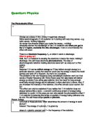
Now when the two types of semi-conductors are combined in a p-n junction, electrical energy can be produced.
In the N-Type there are many electrons (from the phosphorus atoms, having 5 electrons) and in the P-Type there is a deficiency in electrons (from the Aluminium atoms only having 3 electrons), when they are joined electrons from the N-Type diffuse into the P-Type and fill holes near the boundary, leaving holes in the N-Type, near the boundary.
This transferring of electrons leaves a depletion zone near the junction. The silicon is now electrically charges and the N-Type is positive and the P-Type is negative, equilibrium has been reached, thus an electric field is set up, which opposes the movement of electrons from N-Type to P-Type.
Now when a external circuit is connected by metal contacts to the surface of the P and N-Type semi-conductors, and the surfaces are exposed to sunlight, electrons are given energy to jump the energy gap from the valance band to the conduction band, these then flow from the N-Type through the load and then back to the P-Type, completing the circuit. Thus electrical energy, that is able to do work, has been created by the use of the photoelectric effect and semi-conductor properties combined.
- Assess the potential of solar cell technology as an alternative to traditional methods of electricity production.
Solar cells are an excellent alternative energy source. Though it does have pro’s and con’s.
Solar energy is a renewable resource that is environment friendly. Unlike fossil fuels, solar energy is available almost everywhere on earth, the design of the solar cells contain; no liquids, corrosive chemicals or moving parts, they operate silently and have a long life span. This source of energy is also free and it is immune to rising energy prices.
In third world countries, where there is an abundance of sunlight and large rural populations, without the proper infrastructure to develop an electrical grid, solar energy is a very attractive option, its ability to generate electricity at the actual point of use, its low maintenance requirements and its non-polluting technologies.
Already solar energy is important to rural health clinics in developing countries. These clinics require electricity for lighting, vaccine refrigeration and water pumping and purification. Solar energy has proven to be a reliable system for these isolated clinics.
Solar energy is a cost-effective and viable option in many remote areas where power companies may charge anywhere from $18,000-$60,000 a kilometre (depending on terrain) to run a power line to an ‘unserviced’ area.
Though solar energy has its limitations
Not all light is used in this process, most of the sunlight energy cannot be used to free electrons in the solar cells, as it is the wrong frequency and either is reflected or passes through without hitting the electrons.
The electricity attained has a very small electrical potential, even with the most efficient solar cells, therefore they must be chained together in large arrays to be effective enough to provide sufficient energy.
It can only be used during sunny days, it is not suitable for cloudy climates and start up costs are uneconomical.
At the moment solar energy supplies less than 1% of the worlds energy.
Then the most obvious question. What happens when the sun is not shinning?
Though they need to be able to compete with utilities, research is still going on to bring the price of these down though it wont happen for a while yet.
Part of the problem is that manufacturing needs to be done on a large scale to reduce costs as much as possible. This kind of demand for solar energy will not exist until prices fall to competitive levels. Costs are coming down as research is being done and the world is becoming increasingly aware of environmental concerns associated with conventional power sources, making solar energy a technology with a future. Researchers are confident that solar cells will one day be cost effective in urban areas as well as remote areas.
Part 2
- Identify materials that display the properties of a superconductor. Describe the conditions under which they display this behaviour.
When electrons flow through a material there are losses due to resistance. This is a result of electrons colliding with imperfections and impurities in the metal. As the temperature is increased the ions in the lattice vibrate more, this causes a greater chance of electrons colliding and thus more resistance.
But what would happen if we could cool the metal to a point where the ions in the lattice, stopped vibrating?
In 1911, Heike Onnes, a Dutch physicist, discovered that if he cooled mercury to a temperature below 4.2K, its resistance became zero.
This was the first the first insight into superconductivity. A superconductor was later described as an element, metallic alloy, or compound, that will conduct electricity without any resistance when it is cooled to a certain critical temperature. This phenomenon is so useful because with no resistance, there isn't undesirable loss of energy through the material, thus it is more efficient.
There are two types of superconductors:
Type1
- This type of superconductor embodies metals and metalloids that conduct at room temperature. Some examples are mercury, zinc, tin, and lead.
- These were discovered first and require the coldest temperatures to become superconductive.
- There us a very sharp change into a superconducting state.
- They are able to repel a magnetic field completely.
- These loose their superconductivity above a critical value of magnetic field, as the field penetrates the material.
Type 2
- This comprises of metallic compounds and alloys.
- These have a higher critical temperature than Type 1 superconductors.
- The highest critical temperature recorded was 138K
- High magnetic fields also penetrate these materials and cause them to loose their superconductivity.
-
Some examples include YBa2Cu3O7 (YBCO) and Bi2Sr2Ca2Cu3O10.
- Some of these are formed at different pressures and are not chemically stable in some environments.
- Describe current applications of superconductivity.
MRI
Superconductors are used in MRI scanning and are now part of life saving technology. The reason is that doctors need a non-invasive method of finding out what is going on inside the human body. A superconductor produces a strong magnetic field, when conducting a MRI scan, it forces hydrogen atoms, in the water and fat in our bodies, to absorb energy. They then emit energy at a frequency that can be detected, and is then displayed on a computer.
SQUIDS (Superconducting Quantum Interference Device)
When two superconducting materials are separated by a very thin layer of insulator, current flows as Cooper pairs across the insulator – this is the ‘Josephson Effect’. SQUIDS can sense magnetic fields that are billions of times weaker than that which moves a compass pointer. SQUIDS are extensively used in geophysics to measure oscillations in the Earth’s magnetic field.
SQUIDS are used in probing the body by the use of magnetic fields. Research of these is being done in Korea, on Magnetoencephalography (MEG) the imaging of the human brain from magnetic fields. This technology is currently being used and measures the magnetic fields produced by neural activity, and can acquire live footage of the brain structure. The same devices can also be used to monitor magnetic fields from heartbeats.
Magnetic Levitated Vehicles
Very few operate commercially at this moment, though a Sino-German maglev is operating over 30km at Pudong International Airport in Shanghai, China. This transports commuters at extreme speeds, though on average 73 seats are used on each train per week below the maximum capacity of 440. This is because the tickets at this time are too expensive and commuters refuse to pay the high fare.
A test track was built in Japan that is 7km long, these trains are levitated as a result of repulsion. Helium is used to cool superconducting magnets on the vehicle, these magnets interact with the magnetic field around high voltage coils in the guidway. These repell eachother and this causes the train to lift off the track. These train are so good because they eliminate friction, therefore extremely fast travel can be achieved. A 5 carriage train (manned) can hit a top speed of 552km/h.
In the near future these sorts of trains will become more common, though this technology is being held back by political concerns, including the massive cost of construction and environmental concerns of the affect of strong magnetic fields.
- Discuss possible future applications of superconductivity technology
Electricity Transmission and Production
In electrical transmission there are losses due to resistance in the wires, if a ductile superconductor could be manufactured, then this would save enormous amounts of energy and in addition power plants could be built extremely far away from population centres, which reduces environmental and health problems. Though unfortunately the highest temperature superconductors still need to be cooled to a very low temperature and it is not efficient to do such things in long distance cabling, neither is it cost effective. Another thing is that most high temperature superconductors are extremely brittle because they are ceramics. Metal superconductors operate at too low temperatures and need to be cooled by liquid helium that is expensive.
Despite all this there has been tests in Denmark of Superconductor transmission lines, and there are plans for the future. In May of 2001 150,000 residents of Copenhagen, Denmark, received their electricity through HTS (high-temperature superconducting) material. That cable was only 30 meters long, but proved adequate for testing purposes.
More efficient electrical generators can be manufactured if superconducting wire is used rather than the conventional copper wire. If superconducting wire was made into loops, when large currents flow a powerful electromagnet would be set up that would be very effective in a motor or generator as long as it stays below its critical temperature. The efficiently would be well above 99% and their size would half that of normal generators.
Electronic Switches
Fast computers rely of switching between current highways using transistors made from semiconductors. Superconducting devices can be designed to pass a fixed current with barley any driving voltage. The idea is to manufacture computers that are up to 200 times faster than conventional high-speed computers.
The problem of cooling these devices to their critical temperature still exist, and higher temperature superconductors need to be found that are more suited to their applications. The ideal superconductor would need to be ductile, have a critical temperature much higher than the current and arechemically stable in a variety of environments.