- OR – The OR gate is similar to the AND gate in that it again has two input values. This time however if there is an input of 1 at least once then the output will be one. The only time the output will be zero is when both values are zero on input. This is an exact reverse of the AND gate.
- NAND – The NAND logic gate tends to give a only a high voltage output unless both inputs are high voltage in which case a low voltage will be given.
- NOR – The NOR gate is again a reversal of the previous gate, the NAND. In this circumstance when inputs contain a high voltage the output will definitely be a low voltage. If both inputs are low then the output will be high
-
EOR – EOR is standardised form for saying exclusive disjunction. This type of logic gate will give a high output either, but not if both of its two inputs are high. To show this operation the following symbol is used, . Here is the truth table for the EOR logic gate.
- ENOR – This gate again does the opposite to the EOR gate. It will give a low output if either, but not both of its two inputs are high.
Adding numbers in a computer system is often done on the processor in the Arithmetic Logic Unit, this will be described later. But if we wish to use binary values we can sue a form of logic gate called an adder, there are two types of adder, half and full. The half adder is a logical circuit that performs an addition operation. The half adder produces a sum and a carry value which are both binary digits. It uses the following equation;
S = A B
C = A . B
Here is the logic table
Below can be seen the representations used for the logic gates in drawing form.
Registers
Computer processors are made up of many temporary storage areas known as registers. They are not part of the computers memory but are considered to be an additional storage location that helps in maintaining fast speeds. These registers form the most common of computer architecture and operate on the principle of moving data from the main memory, operating them, and then sending them back, giving them a memory location. This is a form of volatile storage.
There are many types of registers found within the CPU but the following are the most common;
- The instruction register – When a programme is to be executed it is toted in to the instruction register, the instruction register has a duty of then splitting the operand register and the address storage register (an example of the operand is when considering a sum, 3 + 3, the threes are operators and the + an operand). It is vital that this process is undertaken because it is the operand part of the instruction that holds the command to be taken
- The sequence control register – This holds the values in which determines what instruction is to be carried out next. This is in the form of a programme counter and can therefore increment the values by 1
- An accumulator – This collects the results of computations
- An address register – Each memory location is notated by an address, the address register stores this so it can find instructions or pieces of data stored in main memory
- A storage register – This temporarily stores data that is from or about to be sent to main memory
It is possible to see that the biggest link to the registers in the CPU is memory. This is because processes come to and from the memory in order to be processed. Each of these registers therefore plays a large part in the way in which the fetch decode and execute cycle takes place.
Busses
A bus system is a series of interconnecting electrical devices which carries signals around a computer system. It is important to break the bus system down into smaller segments as information travels on a number of routes to a specific destination. Below ca be seen the breakdown of the bus system;
- The internal bus – This connects all computer components to the CPU and main memory
- The system bus – This connects the CPU to the level 2 cache
- External bus – Allows expansion boards and memory
It is possible to categorise busses in to certain functions and there are three main types of bus present within a computer system, the three differing bus types are as follows
Address Bus – The address bus is used to connect to the CPU to exact places in the memory locations. The number of wires varies either 32 or 64, the more wires that the bus connects means the more locations it can point to.
Data Bus – The data bus is used for the sending of information across a computer system. When the processor wishes to transmit or receive data it will set the address bus pins appropriately in order for the data bus to work effectively.
Control Bus – The control bus is extensive and is found at all parts of the computer system. It is present in the input output devices, main memory, disk space, and ultimately the CPU. The idea of the control bus is to manage the electrical signals and ensures that data will arrive efficiently in the order in which it was sent.
It is therefore possible that we can consider the CPU to be like a bus station. All information that is passed through the system must go through the CPU as all busses would go through the bus station.
All busses have their variations and properties that make them specific and these properties are measured by
- Bus size
- Clock Speed
- Location
The way in which a bus can send information can be seen in two ways, they are Direct memory access and Bus Mastering. These two methods shall be described in more detail below.
Direct Memory Access – The idea behind direct memory access is to avoid the intervention of the processor allowing computer peripherals to communicate with the memory in order to read or write instruction sets.
Bus Mastering – This process is used to sufficiently increase the performance of the system. The bus takes the form of the processor communicating directly with other devices.
Control Unit and Arithmetic Logic Unit
It can be said that the control unit is the brain within a brain. The CPU is in charge of all the system and is how it functions. But what is it that controls the CPU? This is the control unit. Depending on system setup and what processor is being used ultimately impacts on the control unit to be used.
The control unit is in charge of the Arithmetic logic unit which is in turn responsible for calculating arithmetic operations. It is considered a fundamental building block of the control unit of the micro processor.
Arithmetic logic units make up many of the worlds processors from very basic to very complex systems. An example of this is the arithmetic logic unit within a watch, something that is always incrementing a certain digit by one every time a second elapses.
The system uses the compatible twos compliment system when performing calculations. It is for this reason that engineers have split the arithmetic logic unit up in to differing stages. One stage is for arithmetic calculation and the other for logic. Some processors can then be split up in to differing arithmetic units, dependant on the mathematical unit to be used. From this derives the separation between fixed point arithmetic units and floating point arithmetic units.
Instruction Decoder – When processing information the CPU needs to decode it. This is controlled by the control unit. Each process contains what is known as opcode and the operand. The opcode is the data within the process and the operand is the way in which it should be processed. This information needs to be decoded by the CPU to be in an understandable form of data.
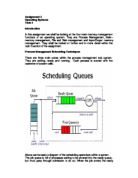
Programme Counter – The programme counter is a vital part of the CPU and is instrumental in how the processor can jump to the next process in the queue. When a process sis finished the programme counter will increment by one and therefore point to the next process to be done. This is ultimately dictated by the operating system, this is because the operating systems scheduling can vary, i.e.) first in first out, round robin and so on.
Memory
The memory used with in a computer micro processor is called cache and this memory type comes in differing levels. The idea of the cache is to reduce the time used to access memory by storing the most commonly used functions and commands within it. Without the cache every time the CPU requested data it would have to go to the main memory to get it. This is very in efficient.
Computers, as I have said consist of two levels of cache and they are level one and level two. Level one however is external to the CPU. Level 2 has greater size meaning that more instructions can be stored within them. The problem with this is that that the more instructions that get stored within means a harder job for the processor to find specific ones. It is still however far greater in efficiency than going directly to the main memory and searching and returning from there.
Bibliography