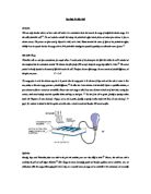
give up electrons. When an electron leave its atom, it leaves behind a hole – or theoretical
equal and opposite charge. A ‘gradient’ is created when ‘p’ and ‘n’ type semiconductors
are juxtaposed, and electrons transfer between them. The ‘gradient’ refers to an electrical
field between the two materials. The loose electron and its hole being to wander down the
gradient, and will eventually cross the junction – or gap. The nature of superconductors will
discourage the electrons from re-crossing, and from the electrons that cross the junction, a
proportion of carriers can be ‘harvested’ by completing a circuit between the cell surface
and the ‘collector’ in the backplane. The current created by the collected electrons passes
electricity to a component such as a heater.
Error! Not a valid filename.
This diagram shows the simplified functioning of a Photovoltaic Cell. Note – there will be
many layers of the specially treated semiconductor material.
Each silicon cell provides a very small amount of electricity. The diagram below
demonstrates how cells can be combined to produce a module, and each module can be
positioned in a solar array – such as we perceive a typical solar panel.
Error! Not a valid filename.
Further components exist in the solar systems to generate electricity efficiently.
* Charge Regulator - Charge regulators are the link between the modules, battery and
load. They protect the battery from overcharge or excessive discharge.
* Battery - Batteries store the energy generated by the solar modules.
* Inverter - Inverters convert DC (direct current) electricity into AC (alternating
current) to run many common appliances and equipment.
Band Gap Theory
‘Band Gap Theory’ is the basis for the functioning of the Photovoltaic cell. Using
layers of oppositely charged semiconductors, the principal of creating an electrical field or
‘gradient’ between the valence band and conduction band allows electrons to ‘jump’ across
the junction and transfer a current through the cell. The energy needed from the photons
striking the semiconductor layers is called ‘photon energy’ and must be at least equal to the
‘band gap energy’ in the covalent bond holding the electrons in place in the valance band.
This diagram illustrates the functioning of a semiconductor in comparison to an insulator or a
metal. In a giant metallic structure (most metals) the ‘gap’ is non-existent; the electrons are
free to travel in a ‘cloud’ or ‘sea’ between the bonded atoms. The opposite is apparent in
an insulator. Here the gap between the valence and conduction bands is too large for
electrons to freely ‘jump’ between them, and so electrical current cannot flow. A
semiconductor however draws a balance between the two extremes. Here, the two bands
are closer together and loose electrons in the valence band are able to ‘jump’ across the
gradient and into the conduction band.
Electrical Characteristics of a Photovoltaic Cell
The characteristics and functioning of a silicon photovoltaic cell depend on the type
and size of load connected to it. Its characteristics will also depend on its own size, and
obviously – the light intensity. In our experiment, we used the same equipment to eliminate
these problems. We also did the entire experiment in one sitting, to keep environmental
conditions at a constant. Other factors such as the heat of the cell will also effects its
conductance.
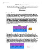
In our experiment, we set up a circuit such as the one below:
When the cell is not connected to any load, there is no current flowing and the voltage
across the PV cell reaches its maximum. This can be seen on the diagram, where the parallel
circuit is simply disconnected. Here, all the current is forced through the voltmeter, which
has a resistance of (20 mega-ohms) accuracy = 0.5% so the resulting current is negligible
(almost 0). Therefore, where R is almost infinite, and current is almost 0, voltage reaches its
maximum. This produces the theoretical EMF of the cell (reading of voltmeter) This is called
the ‘open circuit’. Frequency response of PV cell????
When a load is connected (the variable resistor), the PV cell creates a current and
the voltage goes down. The current reaches a maximum when the two terminals are directly
connected with each other and the voltage is zero. The set-up in this case is called the ‘short
circuit’ and should give the maximum current for the circuit.
Error! Not a valid embedded object.
Error! Not a valid embedded object.
The short circuit and the open circuit are shown as the endpoints of the I-V graph.
This is where resistance is 0 and infinite respectively. For the graphs where light intensity is
lower (such as background light - 393 Lux), the short circuit gave unexpected results.
Where the theory suggests that for infinite resistance, voltage should give the maximum
results; i.e. reflecting the EMF produced, the I-V graphs show a dip for the first result -
where voltage = 0. These unexpected results seem to correct themselves as light intensity
increases, so where Lux = 15050, the short circuit does give maximum current. These
anomalous results may be explained by our recording of the short circuit. Where we noted
every value of potential difference to equal 0, this was not actually the case. We did this due
to time constraints, and without noticing that voltage was not in fact 0. The cause for these
results was a slight resistance, from a reading on the ammeter. This shows that the ammeter
is possibly faulty, as its internal resistance disrupted our results.
The I-V graphs produced by our data seem to follow the model graph (below)
showing a point, where rate of change of gradient is maximum, and a ‘peak power point’ is
produced.
The maximum power point in this graph can also be shown using our own data as a
parabolic curve.
Maximum Power Transfer Theorem
When the impedance of a load connected to a power source is varied from open-circuit to short-circuit,
the power absorbed by the load has a maximum value at a load impedance which is dependent on the
impedance of the power source.
Note that power is zero for an open-circuit (zero current) and for a short-circuit (zero voltage).
Voltage Source
When a load resistance RT is connected to a voltage source ES with series resistance RS, maximum
power transfer to the load occurs when RT is equal to RS.
Under maximum power transfer conditions, the load resistance RT, load voltage VT, load current IT and
load power PT are:
RT = RS
VT = ES / 2
IT = VT / RT = ES / 2RS
PT = VT2 / RT = ES2 / 4RS
Current Source
When a load conductance GT is connected to a current source IS with shunt conductance GS, maximum
power transfer to the load occurs when GT is equal to GS.
Under maximum power transfer conditions, the load conductance GT, load current IT, load voltage VT
and load power PT are:
GT = GS
IT = IS / 2
VT = IT / GT = IS / 2GS
PT = IT2 / GT = IS2 / 4GS
Complex Impedances
When a load impedance ZT (comprising variable resistance RT and variable reactance XT) is connected
to an alternating voltage source ES with series impedance ZS (comprising resistance RS and reactance
XS), maximum power transfer to the load occurs when ZT is equal to ZS* (the complex conjugate of ZS)
such that RT and RS are equal and XT and XS are equal in magnitude but of opposite sign (one inductive
and the other capacitive).
When a load impedance ZT (comprising variable resistance RT and constant reactance XT) is connected
to an alternating voltage source ES with series impedance ZS (comprising resistance RS and reactance
XS), maximum power transfer to the load occurs when RT is equal to the magnitude of the impedance
comprising ZS in series with XT:
RT = |ZS + XT| = (RS2 + (XS + XT)2)½
Note that if XT is zero, maximum power transfer occurs when RT is equal to the magnitude of ZS:
RT = |ZS| = (RS2 + XS2)½
When a load impedance ZT with variable magnitude and constant phase angle (constant power factor) is
connected to an alternating voltage source ES with series impedance ZS, maximum power transfer to the
load occurs when the magnitude of ZT is equal to the magnitude of ZS:
(RT2 + XT2)½ = |ZT| = |ZS| = (RS2 + XS2)½
The place of maximum power on these I-V graphs
http://www.scolar.org.uk/html/school-info/ks4/ks4-2c.html#
Efficiency of cell = 12-15% efficient
For the short circuit when you use EMF for the voltage, and take current you can
find the internal resistance.